LED Strip Quality: Gold Wire, Chip Size and Copper Base Compared
By DENO LED Lighting ·
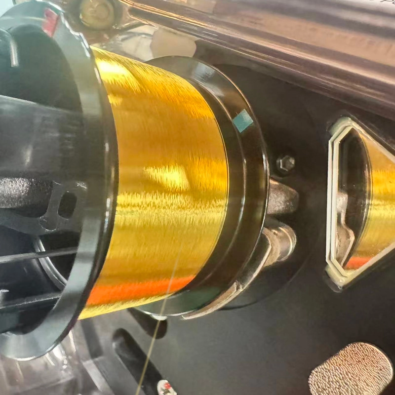
How four LED package construction choices — 99.99% gold bonding wire, gold bump bonding, a 12 x 31 mil die and a silver-plated copper base — affect LED strip quality, and how to verify them in procurement.
Two LED strips can share the same voltage, wattage, CRI and IP rating and still behave very differently after three years in a building. The differences sit inside the LED package: the bonding wire, the bond structure, the chip area and the thermal path out of the die. This article explains the four construction choices DENO makes, what each one does and does not prove, and how to verify them in a supplier audit or a quotation comparison.
1. Bonding wire: 99.99% gold and what it protects against
Inside every encapsulated LED package a hair-thin wire carries current from the chip pad to the lead frame. It is small, it is mechanically loaded every time the package heats and cools, and it sits in whatever atmosphere the encapsulant lets through. DENO specifies 99.99% gold bonding wire in its encapsulated SMD and SOB packages.
The engineering argument for gold is corrosion behaviour, not conductivity alone. Gold is chemically inert: it does not form an oxide layer, and it is far less sensitive to sulphur and chloride contamination than bare copper. That matters most in humid, coastal, cold-room and sealed silicone constructions, where moisture and trace contaminants reach the bond area over years rather than hours.
This is not a claim that copper or alloy wire is unreliable. Bare copper wire has higher electrical and thermal conductivity than gold and is used successfully in very large volumes when the package is engineered for it — inert-atmosphere bonding, controlled bond force and a well-sealed encapsulant. Palladium-coated copper exists precisely to address corrosion. The honest statement is narrower and more useful: gold removes a failure mode that copper packages must control by process, and it does so for the life of the part. For a project that will not be re-lamped for a decade, that is worth paying for; for a two-year retail fit-out it may not be.
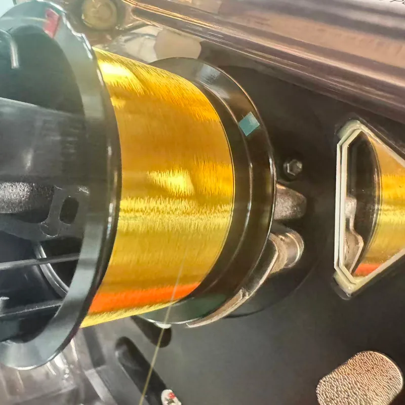
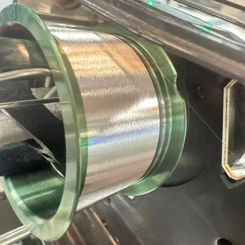
2. Gold bump bonding: the joint, not just the wire
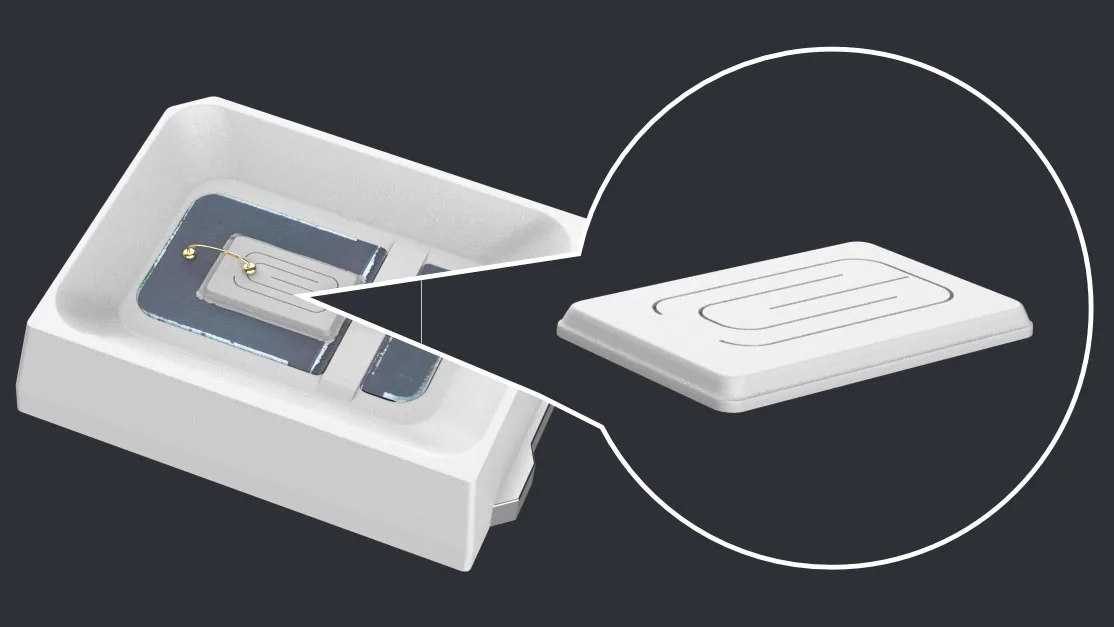
Changing the wire alone does not change the weakest point of the assembly, which is the bond interface on the chip pad. In gold bump bonding a small gold stud is formed on the pad before the wire is attached. The wire is then bonded onto the bump rather than directly onto the pad metallisation.
Two mechanical effects follow. The load-bearing contact area is larger, so shear stress at the interface is lower for the same bond geometry. And the ductile gold bump acts as a compliant layer between the chip and the wire, absorbing part of the strain generated every time the package expands and contracts through a switching cycle. Both effects target bond lift-off, which is a classic wear-out mechanism in packages that see many thermal cycles — stairwells, motion-controlled corridors, refrigerated display and any circuit on a daily timer.
Gold bump bonding is a reliability measure under thermal cycling. It is not a lumen, efficacy or colour-quality improvement, and it should not be quoted as one.
3. Chip area: read the geometry, then read it correctly
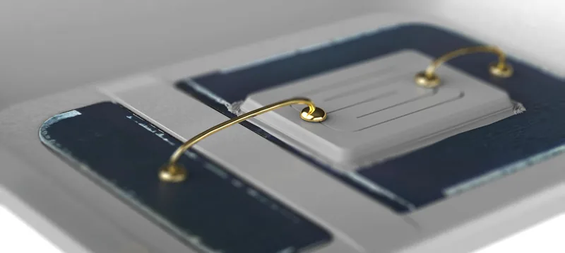
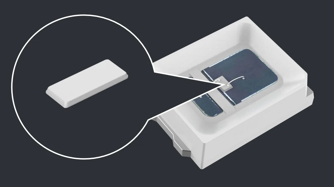
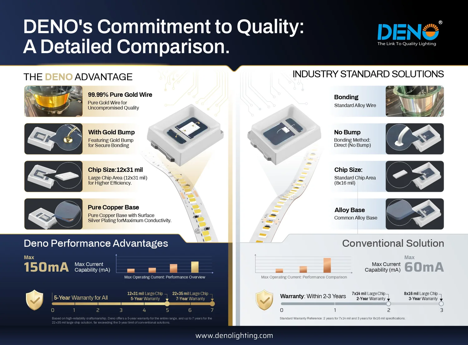
DENO's illustrated package uses a 12 × 31 mil die. Chip dimensions are nominal geometry, so the comparison is simple arithmetic — and it has to be stated against a named baseline, because two different baselines are in common use:
- Against a 7 × 14 mil die: 372 mil² versus 98 mil² — about 3.80 times the nominal area, an increase of roughly 280%.
- Against an 8 × 16 mil die (the baseline printed on the DENO comparison infographic): 372 mil² versus 128 mil² — about 2.91 times the nominal area, an increase of roughly 191%.
What a larger die buys is headroom. At the same drive current, current density per unit of junction area is lower and heat is generated across a wider surface, which reduces local hotspots and gives the package more thermal margin. What it does not buy, automatically, is more light or longer life: luminous flux depends on the epitaxial structure, the phosphor system and the drive current, and lifetime depends on junction temperature in the finished luminaire. An area ratio of 3.80 is never a brightness ratio of 3.80 or a lifetime ratio of 3.80, and any supplier presenting it that way should be questioned.
4. Silver-plated copper base and the complete thermal path
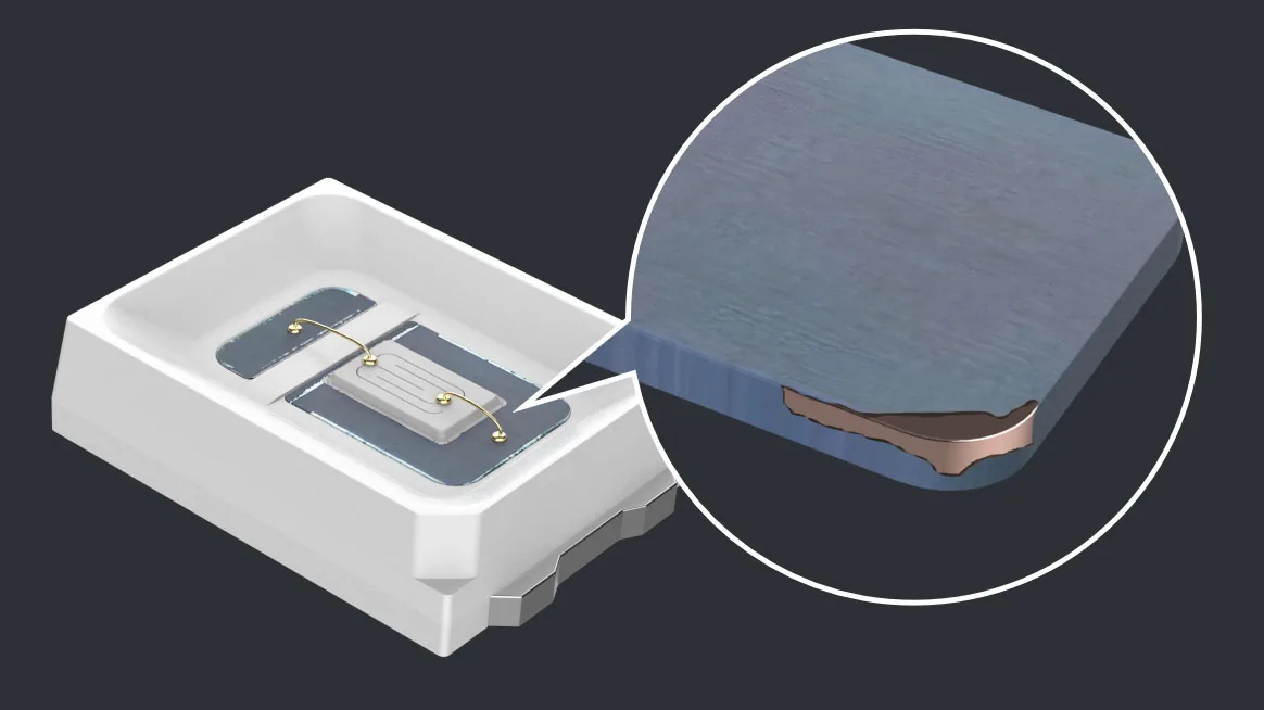
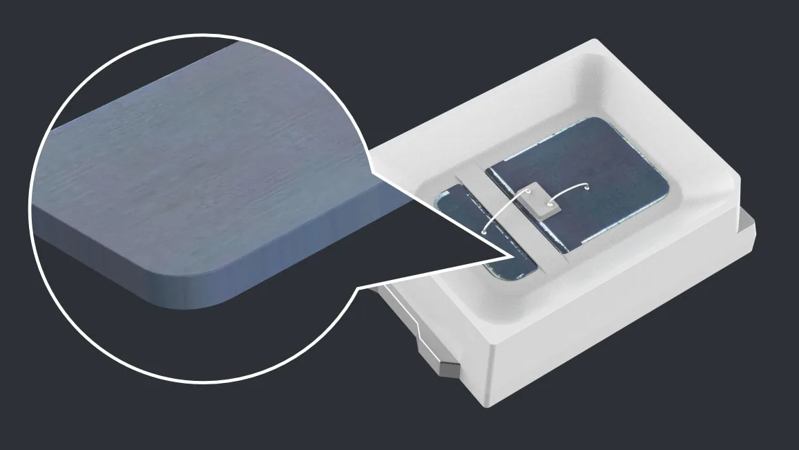
Heat leaves the die through a chain, and the chain is only as good as its worst link: die → die-attach → package base (lead frame or slug) → package solder joint → FPCB copper → adhesive or thermal interface → aluminium profile → surrounding air. DENO uses a pure copper base with silver plating in the illustrated package, and mounts the packages on a thick-copper FPCB — up to 105 µm of copper, with thicker builds available on request — described on the FPCB technology page.
It is worth separating two quantities that marketing material routinely merges. Thermal conductivity is a material property: copper is about 400 W/m·K, aluminium about 200 W/m·K, and common iron-based alloy frames are far lower. Thermal resistance (in K/W) is a property of the finished package and the assembly: it depends on geometry, thickness, die-attach quality, solder coverage and the board underneath. A copper base lowers thermal resistance for a given design, but only measurement of the assembled luminaire tells you the junction temperature you will actually run at. The silver plating exists for solderability and oxidation resistance of the base surface; it is a manufacturing-quality measure, not a separate cooling mechanism.
Practical consequence for specifiers: the copper base is the part of the chain DENO controls in the package, and the FPCB copper weight is the part it controls on the board. Everything after the board — profile, adhesive, cavity ventilation — is controlled on site, which is why higher-wattage builds require an aluminium profile for warranty purposes.
5. Construction comparison
The table below compares construction choices, not measured performance. Each row states what the choice is intended to control; none of them should be read as a guaranteed lumen, efficacy or lifetime figure.
| Construction item | DENO (illustrated package) | Commodity baseline |
|---|---|---|
| Bonding wire Controls corrosion resistance at the bond | 99.99% gold | Alloy or bare copper |
| Bond structure Controls bond lift-off under thermal cycling | Gold bump bonding | Direct wire bond, no bump |
| Die size, nominal Controls current density and heat spreading | 12 × 31 mil = 372 mil² | 7 × 14 mil = 98 mil² (3.80× smaller area) or 8 × 16 mil = 128 mil² (2.91×) |
| Package base Controls thermal resistance die to solder joint | Pure copper, silver plated | Common alloy frame |
| FPCB copper Controls voltage drop and heat spreading | Up to 105 µm, thicker on request | 35 µm (1 oz) RA copper typical |
| Drive current, device Device headroom only, not current per metre | 150 mA maximum for the illustrated device | Lower device rating |
| Warranty Conditional on current, ambient, IP class, profile mounting | 5 years on standard series, subject to the written terms of the specific product | Typically 2–3 years |
Two rows deserve emphasis. The 150 mA figure is the maximum drive current of the illustrated device as printed on the comparison infographic. It is not the current drawn by a metre of finished strip, and it is not a recommended continuous operating point — the operating current for any given series is set by its own photoelectric data. And the warranty row states the standard 5-year term; the specific term for any order is whatever the written warranty for that product says.
6. How to verify LED strip quality in procurement
Construction claims are only worth what the documentation behind them is worth. A short, answerable checklist:
- Bonding wire: ask for the material and purity, and for the package supplier's material certificate.
- Die size: ask for the nominal die dimensions in mil and the baseline used in any comparison figure.
- Package base: ask whether the base is copper or alloy and whether thermal resistance is stated in the package datasheet.
- Board copper: ask for the copper thickness in µm, not in vague terms such as "thick copper", and ask whether it is stated per layer or in total.
- Emitter data: ask for LM-80 data on the emitter, and check that the test current matches the current the strip actually runs at.
- Photometry: ask for integrating-sphere flux, efficacy and chromaticity at the rated current, plus the SDCM bin — DENO supplies SDCM ≤3 as standard, with SDCM 1 available.
- Warranty: read the conditions, not the number of years — rated current, maximum ambient, IP class and profile-mounting requirements decide whether cover survives the first claim.
- Compliance: CE, UL and RoHS documentation confirms compliance; it is not a substitute for batch photometric data.
If two quotations look identical on price, normalise them on delivered lumens per watt at the same CCT and CRI, then compare the answers above. Run the electrical side yourself in the ProCalc engineering suite before deciding, and read the package and board background on the LED chip technology page and the roll-to-roll FPCB page.
7. Frequently asked questions
Is gold bonding wire always better than copper?
No. Gold is chemically inert and removes corrosion of the bond as a failure mode, which is why DENO uses 99.99% gold in its encapsulated packages. Well-engineered copper and palladium-coated copper packages are also reliable, and copper has higher conductivity. The difference matters most in humid, coastal, sealed or long-service installations.
Does a 12 × 31 mil chip produce 280% more light than a 7 × 14 mil chip?
No. 280% is the increase in nominal die area (372 mil² versus 98 mil², a ratio of 3.80). Light output depends on the epitaxial structure, phosphor and drive current. The larger die provides lower current density and better heat spreading, which is a thermal-headroom advantage, not a proportional lumen advantage.
Why do DENO's chip-area figures differ between documents?
Because the baseline differs. Against 8 × 16 mil (128 mil²) the ratio is 2.91× (+191%); against 7 × 14 mil (98 mil²) it is 3.80× (+280%). Always check which baseline a comparison uses before putting the number in a specification.
Is 150 mA the current per metre of strip?
No. 150 mA is the maximum drive current of the single illustrated device. Current per metre depends on the number of LEDs per metre, the circuit topology and the drive voltage, and is given in the photoelectric table of each product.
Does the copper base guarantee a lower junction temperature?
It lowers the package's contribution to thermal resistance, which helps. Junction temperature in service also depends on the FPCB copper, the aluminium profile, the mounting adhesive, the ambient temperature and the drive current, so it has to be evaluated on the finished installation.
Which warranty applies to my order?
The written warranty terms of the specific product ordered. DENO's standard term on its main series is 5 years, conditional on operation within rated current, ambient and IP class, with aluminium profile mounting required above 14 W/m. Warranty periods shown on marketing graphics illustrate specific families and are not a catalogue-wide guarantee.
8. Discuss your project with DENO
For a construction-level comparison against your current supplier, send the target CCT, CRI, wattage per metre, run length, IP class and mounting method. DENO engineering returns the matching series, the photoelectric table, the applicable warranty terms and the documentation package within one business day. Use the contact page for an enquiry, or the OEM/ODM page for private-label and custom board projects.
© All content and images are originally created by DENO and may not be used or reproduced without permission.